Key Takeaways
- Core idea: PCB design turns an electronic schematic into a physical board with components, pads, traces, vias, planes, layers, and manufacturing outputs.
- Engineering use: Engineers use PCB design to make circuits reliable, manufacturable, testable, serviceable, and compact enough for real electronic products.
- What controls it: Component footprints, placement, trace width, clearance, grounding, power distribution, signal speed, thermal behavior, and fabrication limits drive most layout decisions.
- Practical check: A board can pass schematic review and still fail if footprints are wrong, return paths are broken, decoupling is poor, or manufacturing files are incomplete.
Table of Contents
Introduction
PCB design is the process of converting an electronic circuit into a physical printed circuit board layout. It includes schematic capture, footprint selection, component placement, copper routing, board stackup, design-rule checking, and fabrication files so a circuit can be manufactured, assembled, tested, and used reliably.
PCB Design Workflow Diagram
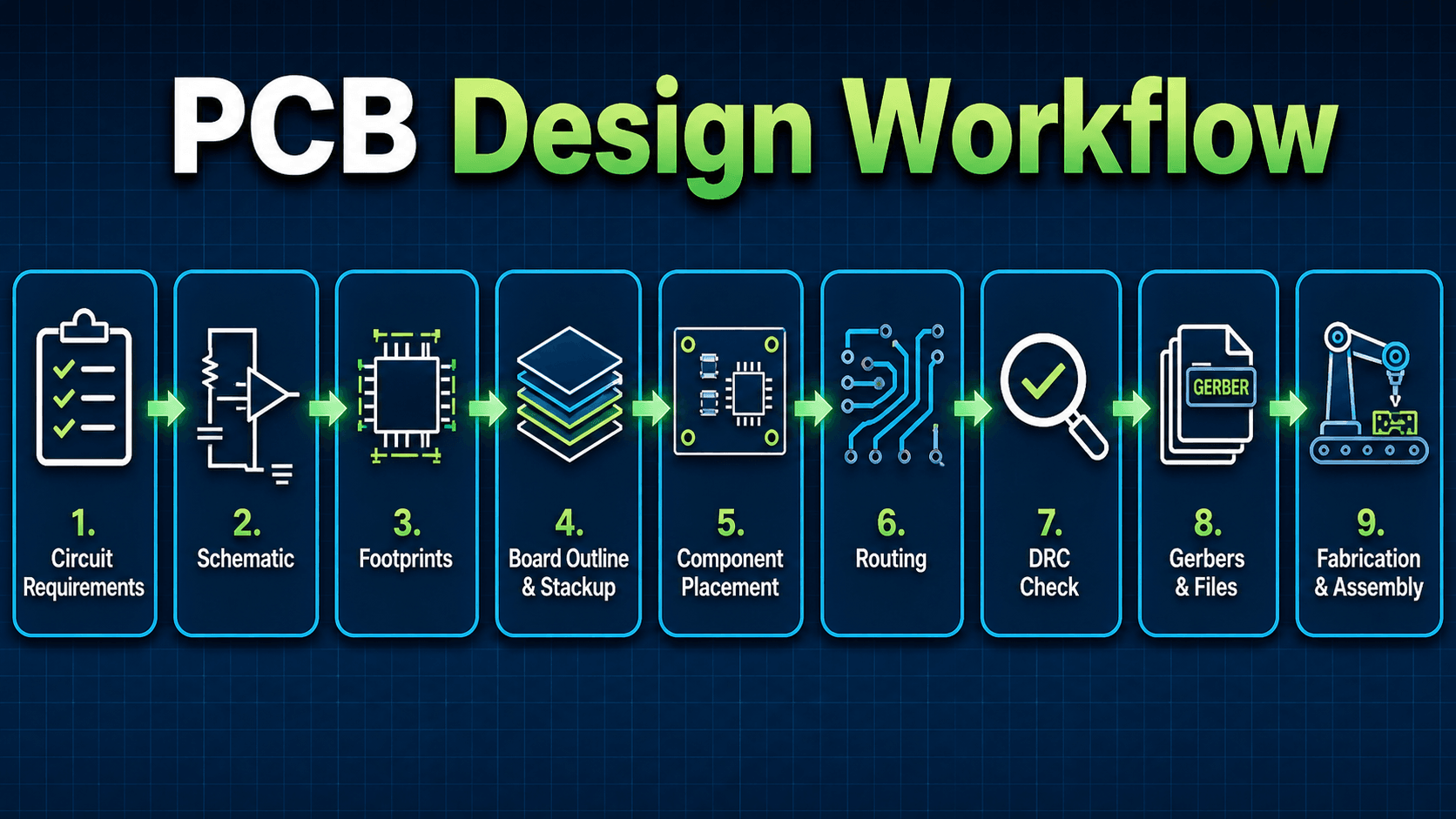
Read the workflow from left to right. The important lesson is that routing is not the first step; good PCB design depends on correct requirements, symbols, footprints, placement, and design rules before copper traces are finalized.
What Is PCB Design?
PCB design is the engineering workflow used to define how electronic components are physically mounted and electrically connected on a printed circuit board. The schematic describes what should be connected; the PCB layout decides where every part sits, how every copper connection is routed, how power and ground are distributed, and how the board will be built.
A useful PCB design is more than a neat drawing. It must satisfy electrical behavior, mechanical fit, manufacturability, test access, thermal performance, connector orientation, serviceability, and cost. That is why a layout that “connects all the nets” can still be a bad design if it has poor grounding, wrong footprints, undersized power traces, or no practical way to assemble and test it.
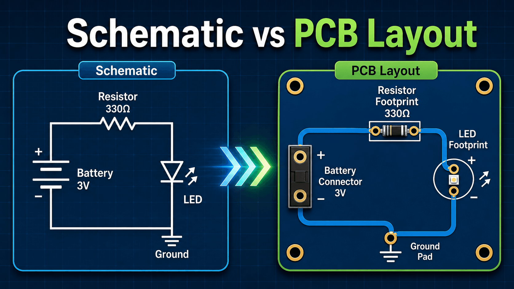
Schematic vs PCB Layout
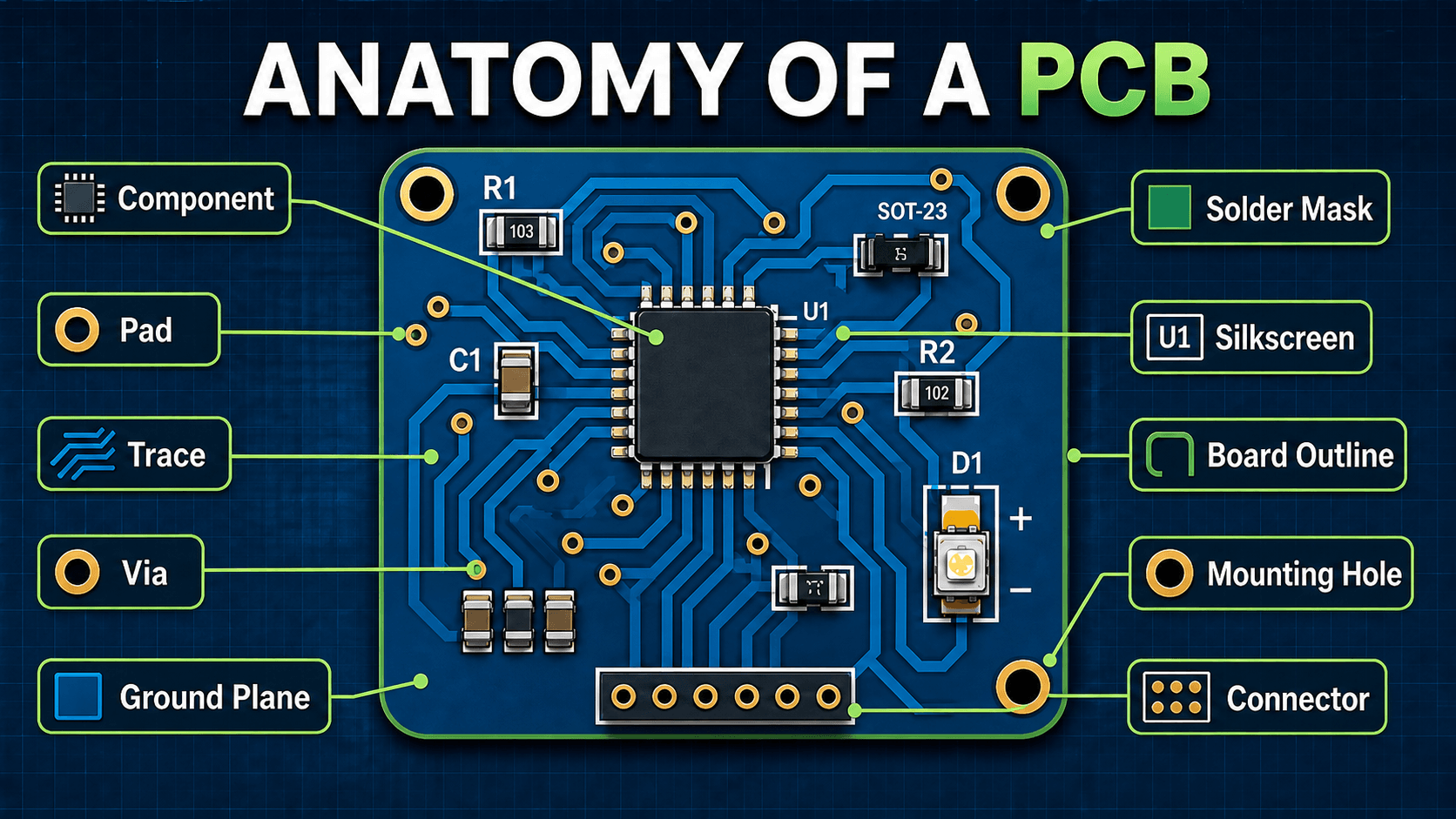
A schematic is the logical circuit map. It shows parts, symbols, pin names, reference designators, and electrical nets. A PCB layout is the physical implementation of that schematic. It turns symbols into real footprints and converts logical nets into copper traces, planes, vias, pads, and assembly information.
Why this distinction matters
Schematic correctness does not guarantee physical correctness. For example, a resistor may be electrically connected to the right net but assigned the wrong package size. A connector may be connected correctly but rotated 180 degrees. A decoupling capacitor may be present in the schematic but placed too far from the IC to be effective.
What transfers from schematic to layout
Nets, reference designators, component values, pin numbers, and assigned footprints transfer into the PCB layout. The designer then makes physical decisions: board size, part position, trace path, via use, copper zones, layer assignment, mounting holes, keepouts, and fabrication outputs.
How PCB Design Works
PCB design works by progressively reducing uncertainty. The early steps define what the circuit must do. The middle steps translate that circuit into physical geometry. The final steps check whether the board can be fabricated, assembled, inspected, and tested without avoidable errors.
1. Define the circuit requirements
Start with voltage levels, current paths, signal types, connector locations, operating environment, enclosure limits, expected production volume, and test needs. These requirements determine whether the board can be simple and low-cost or whether it needs stronger grounding, tighter routing, controlled impedance, thermal relief, or more layers.
2. Create the schematic and assign footprints
The schematic should be reviewed for electrical correctness before layout begins. Each symbol must be paired with the correct footprint, package, pin numbering, polarity, orientation, and land pattern. Footprint mistakes are among the most expensive PCB errors because a board can look professional and still be impossible to assemble.
3. Place components before routing
Component placement controls routing quality. Connectors should line up with mechanical requirements, ICs should be oriented for clean signal flow, decoupling capacitors should sit close to power pins, and high-current or noisy sections should be separated from sensitive analog or low-level signal areas.
4. Route copper and run design checks
Routing connects the nets with copper traces, vias, and planes. After routing, electrical rule checks and design rule checks should catch unconnected nets, spacing violations, drill issues, copper clearance problems, and manufacturing rule conflicts. Gerber review should happen before the board is ordered, not after it arrives.
Key PCB Design Factors
The best PCB layout choices depend on what the board is expected to do. A low-speed LED board, a microcontroller board, a motor driver, an RF board, and a high-current power board all have different layout priorities. The table below summarizes the factors that most often control the design.
| Factor | Why it matters | Engineering implication |
|---|---|---|
| Footprints and pin numbering | The board must physically match the real components being purchased and assembled. | Verify each package against the datasheet before ordering; do not rely only on a library name. |
| Component placement | Placement controls trace length, noise coupling, test access, assembly order, and mechanical fit. | Place connectors, power devices, ICs, and critical passives before routing low-priority signals. |
| Trace width and copper weight | Current-carrying traces generate heat and voltage drop when they are too narrow. | Power traces, LED strings, motor paths, and regulator outputs usually need wider copper than logic signals. |
| Clearance and creepage | Spacing affects manufacturability, isolation, contamination tolerance, and safety margin. | Use manufacturer design limits as a minimum, then increase spacing when voltage, dirt, moisture, or reliability matter. |
| Grounding and return paths | Signal current returns through the reference structure, not through an abstract ground symbol. | Use continuous reference planes where possible and avoid routing important signals over plane splits. |
| Layer count and stackup | Layer count affects routing density, cost, power integrity, EMI behavior, and reference-plane quality. | Use 2 layers for simple low-speed designs; consider 4 layers when grounding, routing density, or noise control becomes important. |
| Manufacturing rules | Fabricators have limits for trace width, spacing, drill size, annular ring, solder mask, and board outline features. | Set design rules to match the intended manufacturer before routing, not after the board is finished. |
Good vs Bad PCB Routing
Routing quality is one of the clearest differences between a beginner board and a production-ready design. Good routing is not just visually tidy; it supports the electrical behavior of the circuit by keeping current paths short, controlling loop area, providing a nearby return path, and separating noisy and sensitive sections.

Power traces need more than electrical continuity
A thin trace may connect a supply net correctly but still cause voltage drop, heating, or unreliable operation. Power traces should be sized for expected current, acceptable temperature rise, copper thickness, and distance. For power converters, motor drivers, LEDs, and battery-fed boards, power-path geometry is often a design driver.
Decoupling capacitors are placement-dependent
A decoupling capacitor is not equally effective anywhere on the same net. It should be placed close to the IC power and ground pins with a short, low-inductance path. If it is routed through long traces or shares a noisy return path, it may not suppress local supply transients when the IC switches.
After routing, follow the actual current path from the power source to each load and back through its return path. If the loop is large, broken by a split plane, or routed around the board unnecessarily, the layout needs review.
2-Layer vs 4-Layer PCB Stackup
Layer count is a design decision, not just a cost decision. A 2-layer board can be excellent for simple low-speed circuits, but it gives the designer fewer options for clean grounding and routing. A 4-layer board adds cost, but it can provide a more continuous ground plane, better power distribution, and cleaner signal return paths.
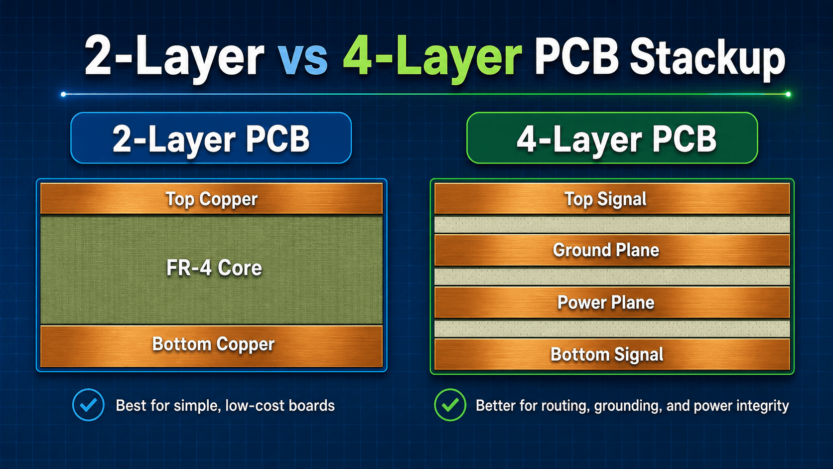
When 2 layers make sense
Use a 2-layer board for simple circuits, low-speed signals, generous board area, low component density, basic sensors, simple LED boards, and early prototypes where cost and fast iteration matter more than high-density routing or signal integrity.
When 4 layers make sense
Use a 4-layer board when the design has dense routing, microcontrollers, mixed analog and digital sections, faster edges, switching regulators, USB or other higher-speed interfaces, noise sensitivity, or tight mechanical space. The cost increase can be justified if it prevents layout compromises that would cause debugging delays or redesigns.
PCB Design Review Checklist
A good PCB review should happen before fabrication files are released. The goal is to catch errors that automated checks miss: wrong footprints, bad connector orientation, missing test access, questionable return paths, and layout choices that pass DRC but fail in real hardware.
Review in this order: requirements first, schematic second, footprints third, placement fourth, routing fifth, manufacturing outputs last. If a later step looks wrong, trace the issue backward instead of patching the layout without understanding the cause.
| Check or decision | What to look for | Why it matters |
|---|---|---|
| Schematic and net review | Unconnected pins, incorrect net names, missing pull-ups, missing protection, wrong supply rails, and unclear connector labels. | The PCB layout can only implement the schematic it is given; schematic mistakes become physical board mistakes. |
| Footprint verification | Package dimensions, pin numbering, polarity marks, connector orientation, thermal pad dimensions, and assembly clearance. | Wrong footprints are one of the most common causes of unusable first articles. |
| Placement review | Signal flow, decoupling location, connector access, mounting holes, enclosure fit, high-current paths, and thermal spacing. | Good placement makes routing easier; poor placement forces compromises that DRC may not flag. |
| Routing and ground review | Return paths, power-trace width, via count, plane cuts, trace length, sensitive analog routing, and noisy switching loops. | A board can be electrically connected but still noisy, unstable, hot, or hard to debug. |
| Manufacturing file review | Gerbers, drill files, solder mask, silkscreen, board outline, BOM, pick-and-place data, and polarity notes. | Fabricators and assemblers build from these outputs, so missing or inconsistent files can delay or ruin the build. |
Do not approve the board only because DRC passes. Open the Gerbers in an independent viewer, inspect every layer, verify orientation marks, check polarity, and confirm that the fabrication and assembly package tells the manufacturer exactly what to build.
Manufacturing Files and Design for Manufacturing
The end product of PCB design is not just a layout file. It is a manufacturing package that communicates the board geometry, copper layers, drill data, solder mask, silkscreen, board outline, materials, component list, and assembly requirements. Good design for manufacturing reduces ambiguity before the board enters fabrication.
Fabrication outputs
Fabrication outputs typically include copper layer Gerbers, solder mask layers, silkscreen layers, paste layers if needed, mechanical or board outline data, drill files, fabrication notes, board thickness, copper weight, finish, and tolerance requirements. These files tell the board house how to fabricate the bare PCB.
Assembly outputs
Assembly outputs usually include a bill of materials, pick-and-place file, assembly drawing, polarity markings, reference designators, and notes for special handling. Assembly data becomes more important when the board has polarized capacitors, diodes, connectors, fine-pitch ICs, bottom-side parts, or parts with thermal pads.
Do not assume the manufacturer can infer intent from the PCB image. If polarity, connector orientation, component substitutions, stackup, or special assembly requirements matter, they should be clearly represented in the output files and notes.
Engineering Judgment and Field Reality
Real PCB design includes tradeoffs that do not show up in a simple tutorial. The cheapest board is not always the lowest-cost product if it creates redesigns, unstable operation, heat problems, assembly scrap, or field failures. The best layout is usually the one that balances performance, manufacturability, inspection, enclosure fit, repairability, and schedule risk.
Experienced designers also think about how the board will be debugged. Test points, readable silkscreen, logical connector labels, accessible measurement nodes, and clear ground references can save hours during bring-up. A board with no test access may be technically compact but difficult to validate when the first prototype does not behave as expected.
The first prototype often reveals problems that the CAD tool cannot know: wrong connector mating direction, heat near plastic parts, silkscreen hidden under components, inaccessible test pads, awkward cable strain, or a part that is technically correct but unavailable in the required package.
When This Breaks Down
Basic PCB design guidance works well for simple boards, but it starts to break down when signals become fast, currents become high, voltages become hazardous, noise margins become tight, or the board must pass formal environmental, reliability, or electromagnetic compatibility requirements.
- High-speed designs: Fast digital edges may require impedance control, length matching, continuous reference planes, careful via transitions, and connector-level signal integrity review.
- High-current designs: Motor drivers, LED power boards, battery systems, and regulators may require copper pours, thermal vias, wider traces, heat spreading, and current-loop control.
- Mixed-signal boards: Sensitive analog measurements can be disrupted by digital return currents, switching regulators, poor reference routing, or noisy ground connections.
- High-voltage boards: Clearance, creepage, insulation, contamination, and safety requirements can dominate the layout more than ordinary trace routing.
- Production assemblies: Panelization, fiducials, pick-and-place data, solder paste apertures, reflow profile, inspection, and component availability become part of the design problem.
Common PCB Design Mistakes
Many PCB failures are not caused by one complex theory mistake. They are caused by small practical misses that compound: a rotated connector, a weak ground return, a missing test point, an undersized trace, or a footprint copied from the wrong package variant.
- Using the wrong footprint: Always check pad dimensions, pin order, polarity, and mechanical fit against the actual part datasheet.
- Routing before placement is stable: If placement is poor, routing becomes a workaround instead of a design.
- Ignoring return current: Signals need a nearby return path, especially when edges are fast or loops are large.
- Placing decoupling capacitors too far away: Decoupling is most effective when the current loop is short and direct.
- Using manufacturer minimums everywhere: Minimum trace and spacing rules are fabrication limits, not always reliability or performance best practices.
- Forgetting board bring-up: Add test points, readable labels, and accessible ground references before the board is released.
- Skipping Gerber inspection: A layout screenshot is not a substitute for checking the exact files the manufacturer will use.
The most damaging beginner mistake is treating PCB layout as automatic wire drawing. PCB design is physical engineering: copper geometry, component placement, return paths, heat, assembly, and manufacturing constraints all affect whether the board works.
Useful References and Design Context
PCB design is commonly performed in electronic design automation software, but the underlying workflow is the same: schematic capture, footprint assignment, board layout, rule checking, and manufacturing output review. Tool documentation is useful because it shows how these stages connect in a real design environment.
- KiCad documentation: KiCad Getting Started documentation for schematic and PCB design workflow explains an integrated workflow for creating schematics, printed circuit boards, and related design outputs.
- Project-specific criteria: PCB manufacturers, assembly houses, owner requirements, enclosure constraints, safety expectations, and component availability can all control final layout choices.
- Engineering use: Designers use CAD documentation, fabrication capabilities, assembly rules, and project constraints together when deciding trace widths, clearances, stackups, footprints, file outputs, and review steps.
Frequently Asked Questions
PCB design is the process of converting an electronic schematic into a manufacturable printed circuit board layout. It includes selecting footprints, defining the board outline, placing components, routing copper traces, adding planes, checking design rules, and generating files for fabrication and assembly.
A schematic shows the logical electrical connections between components, while a PCB layout shows the physical board, footprints, pads, traces, vias, layers, and mechanical constraints. A schematic can be electrically correct but still become a poor PCB if placement, routing, grounding, or manufacturability are handled badly.
A beginner can start with a 2-layer PCB for simple low-speed circuits, especially when cost and learning are the priority. A 4-layer PCB becomes more useful when the design needs better grounding, cleaner power distribution, smaller routing space, lower noise, or more predictable signal return paths.
A basic PCB fabrication package usually includes Gerber files, drill files, a board outline, solder mask layers, silkscreen layers, and fabrication notes. If the board will be assembled by a manufacturer, the package usually also needs a bill of materials, pick-and-place file, assembly drawing, and polarity or orientation notes.
Summary and Next Steps
PCB design is the practical bridge between circuit theory and physical electronics hardware. It turns a schematic into a board that can be fabricated, assembled, tested, and installed in a real device.
The most important design decisions are not only the trace routes. Footprints, placement, return paths, grounding, power distribution, layer stackup, manufacturing limits, and review discipline all determine whether the final board works reliably.
Where to go next
Continue your learning path with related Turn2Engineering resources.
-
Basic Electronic Components
Review the resistors, capacitors, diodes, transistors, ICs, and connectors that become real footprints on a PCB.
-
Circuit Analysis
Strengthen the electrical foundation behind voltage, current, power, and circuit behavior before turning a schematic into a board.
-
PCB Layout Tools
Learn how design software supports schematic capture, layout, routing, checks, visualization, and manufacturing file generation.