Key Takeaways
- Core idea: Rapid prototyping in electronics is the fast build-test-iterate process used to validate circuits, PCBs, firmware, and product assumptions before production.
- Engineering use: It helps engineers find schematic, layout, thermal, firmware, connector, and manufacturability problems while changes are still relatively inexpensive.
- What controls it: The best prototype method depends on circuit speed, current, noise sensitivity, mechanical fit, test access, cost, and how close the design is to production.
- Practical check: A useful prototype should test a specific risk with expected measurements, pass/fail criteria, and a clear decision for the next design revision.
Table of Contents
Introduction
Rapid prototyping in electronics is the process of quickly turning a circuit concept into a physical or simulated prototype so engineers can test function, performance, layout, firmware, and manufacturability before final production. In electronics, this often means moving from simulation or breadboard testing into a quick-turn PCB prototype that can reveal grounding, thermal, connector, and manufacturing issues.
Rapid Prototyping Workflow in Electronics
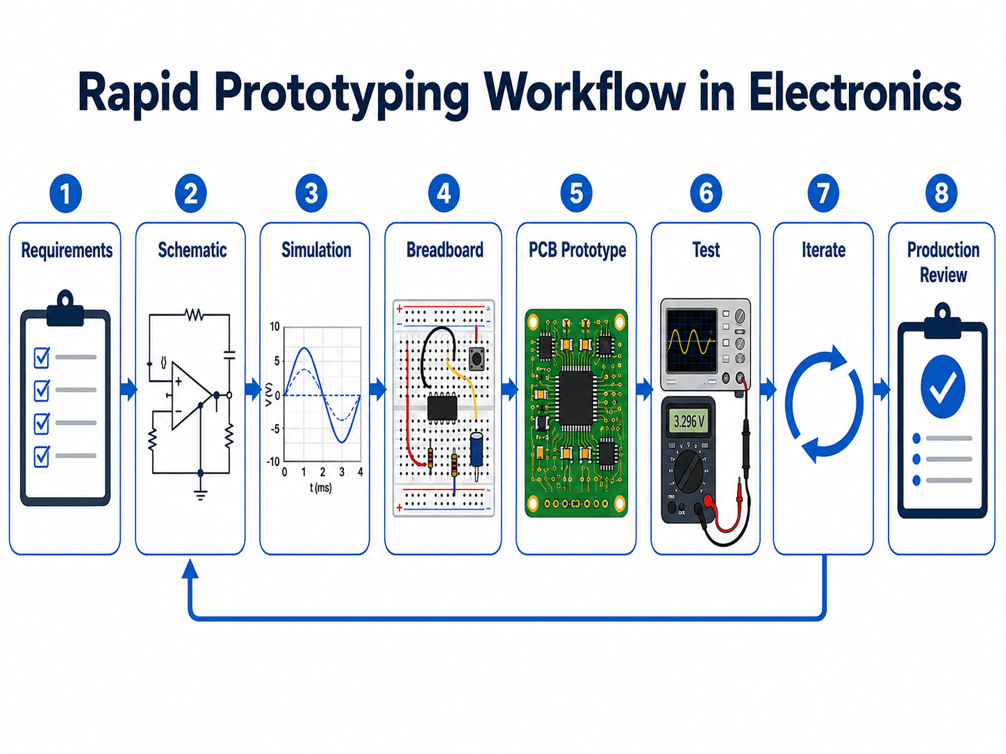
Notice that the loop returns from testing and iteration back to earlier design stages. That feedback path is what separates disciplined engineering prototyping from simply building something quickly.
What Is Rapid Prototyping in Electronics?
Rapid prototyping in electronics is a compressed development workflow used to test an electronic design before it is locked for production. It may start with a simulated circuit, move to a breadboard or evaluation module, advance into a quick-turn PCB, and eventually become an engineering validation build that resembles the final product.
In practical electronics engineering, the purpose of a prototype is to answer a design question. Can the power supply handle the load? Does the sensor interface behave as expected? Is the microcontroller pinout correct? Does the PCB layout introduce noise? Can the board be assembled and tested repeatedly? A useful prototype gives evidence, not just a working demo.
Rapid prototyping is broader than ordering a fast PCB. It includes schematic capture, circuit simulation, breadboarding, firmware bring-up, connector checks, thermal testing, signal measurement, component substitution, and design-for-manufacturing review. The faster the loop, the sooner engineering teams discover which assumptions were wrong.
Why Rapid Prototyping Matters for Circuit and PCB Design
Electronic designs can fail for reasons that are not obvious in a clean schematic. A regulator may overheat because the copper area is too small. A digital interface may pass a logic check but fail due to ringing, timing margin, or poor grounding. A connector may be electrically correct but mechanically impossible to reach inside the enclosure. Rapid prototyping exposes these problems early.
The biggest value is risk reduction. Instead of waiting until a production build to discover footprint errors, missing test points, noisy analog inputs, or firmware programming issues, engineers create smaller validation loops. Each loop should test one or more risks and produce a design decision.
| Prototype risk | What the prototype reveals | Why it matters before production |
|---|---|---|
| Electrical function | Whether the circuit performs the intended switching, sensing, amplification, conversion, or control behavior. | Functional errors are easier to fix before PCB layout, tooling, documentation, and production commitments are made. |
| Layout-dependent behavior | Noise, ripple, coupling, impedance, current path, grounding, and high-speed signal problems. | These issues often do not appear on a simple breadboard or idealized simulation. |
| Firmware and hardware integration | Boot mode, programming access, pin assignments, communication timing, interrupt behavior, and debug visibility. | Many embedded failures come from the boundary between hardware and code, not from either one alone. |
| Manufacturability | Footprint accuracy, solderability, assembly access, connector orientation, test access, and documentation gaps. | A board that works once on a bench may still be hard to build, inspect, or repair at scale. |
Before starting a prototype, write down the specific decision it must support. “Build a prototype” is vague; “verify the 3.3 V rail under peak radio transmission current” is testable.
Rapid PCB Prototyping: Where the Design Becomes Real Hardware
Rapid PCB prototyping is the point where the design starts behaving like real hardware instead of a temporary circuit. A prototype PCB uses the actual board outline, component footprints, copper routing, planes, connectors, mounting holes, and fabrication constraints that affect electrical and mechanical performance.
This is where PCB design decisions become visible. Ground returns, decoupling placement, copper width, thermal relief, connector orientation, signal routing, and test access can all change how the prototype behaves compared with a breadboard or simulation.
| Rapid PCB item | What it includes | Engineering reason it matters |
|---|---|---|
| Schematic and netlist | The logical circuit connections that drive PCB layout. | Errors here usually propagate directly into the board unless caught by review or electrical rule checks. |
| PCB layout | Component placement, routing, planes, board outline, clearances, and mounting features. | Layout determines many real-world behaviors: noise, current paths, heat spreading, and connector access. |
| Gerber and drill files | The fabrication data used to make copper layers, solder mask, silkscreen, and holes. | A clean Gerber package reduces fabrication delays and helps catch layer, polarity, or drill issues before ordering. |
| BOM and assembly data | Component list, package information, pick-and-place files, and assembly notes. | Prototype speed is limited if parts are unavailable, mismatched, incorrectly oriented, or poorly documented. |
| Bring-up plan | Inspection, current-limited power-up, rail checks, firmware programming, interface tests, and load tests. | The first power-up should be controlled and measurable, not a blind “plug it in and hope” event. |
Inspect the board → check for shorts → apply current-limited power → verify each rail → confirm clock/reset behavior → program firmware → test interfaces → apply realistic loads → record issues for the next revision.
Common Electronics Prototype Methods
The right prototyping method depends on what the engineer needs to learn. A breadboard is fast and cheap for simple low-speed circuits, but it does not behave like a finished PCB. A quick-turn PCB takes more setup effort, but it gives a much better view of layout-dependent electrical behavior, assembly constraints, and product packaging.
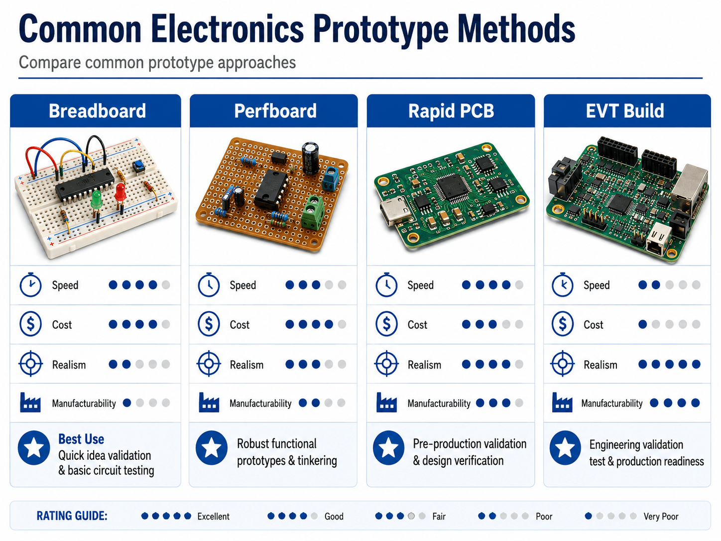
Breadboard prototypes
Breadboards are best for low-speed concept checks, simple sensor circuits, logic experiments, and early component selection. They are useful when the question is “does this circuit idea work at all?” They are not reliable for high-current, high-frequency, RF, precision analog, low-noise, or thermally sensitive designs.
Perfboard and hand-wired prototypes
Perfboard creates a more durable prototype than a breadboard while still allowing hand assembly and quick changes. It is useful for one-off functional builds, but it usually does not represent the final PCB layout, controlled impedance, manufacturability, or automated assembly process.
Rapid PCB prototypes
A rapid PCB prototype uses actual board layout, footprints, traces, planes, connectors, and mounting features. This is the preferred method when the design question involves grounding, trace routing, decoupling, mechanical fit, test points, thermal performance, or manufacturing handoff.
Engineering validation builds
An EVT-style build is closer to the product intent. It may include enclosure fit, full firmware, representative connectors, manufacturing documentation, and a structured test plan. It is slower and more expensive than a breadboard or quick PCB, but it answers higher-value questions about repeatability, reliability, and production readiness.
Electronics Prototype Stages: POC, Functional, EVT, DVT, and PVT
Prototype terminology can be confusing because teams use different words depending on whether they come from engineering, manufacturing, startup product development, or electronics assembly. The key is to understand what each stage is trying to prove.
| Prototype stage | Main purpose | Typical electronics output |
|---|---|---|
| Proof of concept | Prove that the basic circuit or product idea is possible. | Simulation, breadboard, breakout board, evaluation module, or rough bench setup. |
| Functional prototype | Validate the main electrical function under controlled conditions. | Perfboard, early PCB, firmware demo, or simple enclosure mockup. |
| Engineering validation test build | Test product-like electrical, firmware, mechanical, and thermal behavior. | Representative PCB assembly with connectors, firmware, debug access, and structured test plan. |
| Design validation test build | Verify that the design meets user, environmental, interface, and reliability expectations. | More complete hardware with closer-to-final enclosure, firmware, cables, and operating modes. |
| Production validation test build | Confirm that the manufacturing process can repeatedly build the design. | Production-intent PCB assembly, documentation, test fixtures, inspection criteria, and process checks. |
Early prototypes are about learning quickly. Later prototypes are about repeatability, documentation, manufacturability, and confidence that the design can survive real product constraints.
Rapid Prototyping vs Traditional Electronics Prototyping
Traditional electronics prototyping often follows a slower, more sequential path: design, build, test, revise, and then repeat after a long delay. Rapid prototyping compresses that loop by using simulation, modular test circuits, quick-turn PCB services, reusable evaluation boards, and faster feedback between electrical, firmware, mechanical, and manufacturing teams.
| Comparison point | Traditional prototyping | Rapid prototyping in electronics |
|---|---|---|
| Iteration speed | Longer cycles between design changes and tested hardware. | Shorter loops using simulation, breadboards, modules, and quick-turn PCB builds. |
| Design learning | Problems may appear late after a more complete design is built. | Specific risks are isolated and tested earlier. |
| Documentation pressure | Documentation may be more formal but slower to update. | Documentation must stay lightweight but accurate so fast changes are not lost. |
| Main risk | Slow discovery of design problems. | False confidence if speed replaces review, measurement, and pass/fail criteria. |
When to Move from Breadboard to PCB Prototype
Breadboards are excellent for early learning, but they eventually become the wrong tool. The design should move toward a PCB prototype when wiring parasitics, mechanical constraints, power integrity, thermal behavior, connectors, or repeatable testing become part of the design risk.
| Design condition | Stay with breadboard if… | Move to PCB prototype if… |
|---|---|---|
| Signal speed | The circuit is low-speed and tolerant of long jumper wires. | Edge rates, clock signals, communication buses, RF behavior, or waveform shape matter. |
| Power delivery | Current is low and voltage drop is not a major concern. | Regulators, motors, radios, LEDs, heaters, or pulsed loads create current and thermal risk. |
| Analog performance | The goal is a rough proof-of-concept. | Noise floor, offset, filtering, shielding, grounding, or sensor accuracy affects the result. |
| Mechanical fit | Form factor does not matter yet. | Connector placement, mounting holes, enclosure clearance, or cable routing must be verified. |
| Manufacturing readiness | The prototype is only for exploration. | The team needs to evaluate footprints, assembly process, test points, fabrication files, and the bill of materials. |
A breadboard can prove a concept and still hide the problem that will break the real board. Long jumper wires, loose contacts, missing ground planes, and unrealistic power paths can make the prototype both less stable and less representative than a PCB.
What Engineers Test on an Electronics Prototype
Testing is where rapid prototyping becomes engineering rather than trial-and-error. A prototype should be measured against expected behavior: voltage levels, current draw, ripple, timing, signal quality, temperature, firmware behavior, connector pinout, and mechanical fit. The goal is to learn whether the design margin is real.
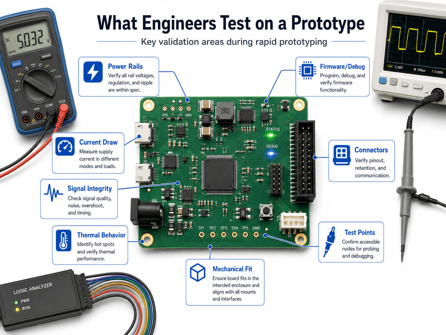
Power rails and current draw
The first checks are usually supply voltage, startup behavior, ripple, current in each operating mode, and response to peak load. A board can appear to work at idle and still fail when a radio transmits, a motor starts, or firmware enables several loads at once.
Signal integrity and timing
Oscilloscopes, logic analyzers, and protocol tools help verify waveform quality, timing, rise and fall times, noise, overshoot, ringing, and bus communication. This is especially important for digital electronics, mixed-signal boards, sensors, high-speed interfaces, and precision analog circuits.
Firmware and debug access
Embedded prototypes need programming headers, boot-mode access, reset control, debug pins, and enough test visibility to diagnose problems. A missing programming header or blocked debug connector can turn a simple firmware issue into a board re-spin.
Mechanical and thermal behavior
Engineers also check whether the board fits the intended enclosure, whether connectors are accessible, whether mounting holes align, and whether heat-producing components have enough copper area or airflow. Thermal problems are often easier to identify on a PCB than on a breadboard.
Senior Engineer Prototype Review Checklist
A strong prototype review asks whether the next build will teach the team something useful. The checklist below is designed for electronics prototypes that are moving from concept, simulation, or breadboard work toward a PCB prototype or validation build.
Define the risk → review the schematic → check layout and footprints → confirm BOM availability → plan test access → bring up power safely → measure expected behavior → document changes before the next iteration.
| Review area | What to look for | Why it matters |
|---|---|---|
| Prototype objective | A written statement of what the prototype must prove, measure, or eliminate as a risk. | Without a defined objective, teams may confuse a demo with a validated design. |
| Schematic readiness | Power sequencing, decoupling, pullups, reset circuits, protection devices, connector pinout, and IC support components. | Schematic mistakes can make the PCB impossible to debug, even if the layout is clean. |
| Footprints and packages | Pad dimensions, pin numbering, polarity marks, connector orientation, package variants, and alternate parts. | Wrong footprints are one of the fastest ways to lose a prototype build. |
| Layout and routing | Return paths, plane continuity, trace width, spacing, thermal paths, sensitive analog routing, and high-current loops. | Layout turns a correct schematic into either a reliable board or a noisy, fragile one. |
| Test access | Power test points, ground clips, programming headers, debug pads, probe clearance, and labeled nodes. | Testing must be designed into the board; it is difficult to add after fabrication. |
| Firmware bring-up | Boot pins, reset behavior, programming path, UART/SWD/JTAG access, status indicators, and safe default outputs. | Embedded boards need a planned path for programming, logging, and recovering from firmware errors. |
| Manufacturing handoff | Gerbers, drill files, assembly drawings, BOM, pick-and-place data, fabrication notes, and known design risks. | Rapid PCB fabrication still needs clean documentation or the prototype may be delayed or assembled incorrectly. |
Review the prototype before ordering boards, not after. A 20-minute footprint, connector, and test-point review can prevent days or weeks of rework.
PCB Prototype File Package Checklist
Quick-turn PCB prototyping depends on clean files. Fast fabrication does not help if the design package is incomplete, ambiguous, or internally inconsistent. A good prototype file package should make it clear what the board is, how it is fabricated, how it is assembled, and how the first article will be tested.
| File or document | What it controls | Prototype QA check |
|---|---|---|
| Gerber files | Copper layers, solder mask, silkscreen, paste, board outline, and fabrication details. | Open the exported files in a Gerber viewer and compare them against the intended board stack and outline. |
| Drill files | Plated and non-plated holes, vias, mounting holes, and connector holes. | Confirm hole sizes, plated status, and mechanical mounting features before fabrication. |
| Bill of materials | Part numbers, quantities, references, packages, manufacturer data, and alternates. | Check availability, lifecycle status, package match, and substitutions for critical parts. |
| Pick-and-place file | Component placement, rotation, and side of board for assembly. | Review rotations for ICs, diodes, electrolytic capacitors, connectors, and polarized components. |
| Assembly drawing | Reference designators, polarity marks, connector orientation, special instructions, and do-not-populate notes. | Make sure an assembler can build the board without interpreting intent from the schematic. |
| Revision notes | What changed, known risks, test objectives, and unresolved issues. | Document what the prototype is supposed to prove and what should be checked first during bring-up. |
Rapid PCB Prototyping and Manufacturing Readiness
A quick-turn PCB is still a manufacturing package. The board house and assembler need enough information to fabricate, inspect, and populate the board correctly. That means prototype speed should not replace basic design-for-manufacturing discipline.
Good rapid PCB prototyping connects PCB layout tools, component libraries, bill-of-material checks, design rule checks, assembly notes, and test planning. It also prepares the design for later design for manufacturing in electronics.
| Manufacturing item | Prototype concern | Practical review question |
|---|---|---|
| Gerber and drill files | Fabricator must receive the exact copper, solder mask, silkscreen, and hole information. | Were the exported files reviewed in an independent Gerber viewer? |
| Bill of materials | Prototype parts may be unavailable, obsolete, package-mismatched, or expensive in quantity. | Are alternates identified for critical or hard-to-source components? |
| Assembly data | Pick-and-place files, polarity, reference designators, and assembly drawings drive correct board population. | Can an assembler determine orientation without guessing? |
| Test strategy | Manufacturing test is difficult without access to important nodes and clear pass/fail criteria. | Can power, firmware, communication, and key signals be checked without special rework? |
Common Causes of PCB Prototype Re-Spins
A PCB re-spin is not always a failure. It is often part of learning. The problem is preventable re-spins caused by issues that could have been caught with better review, file checking, or test planning.
| Re-spin cause | Typical symptom | How to reduce the risk |
|---|---|---|
| Mirrored or rotated connector | Cable does not fit, pinout is reversed, or enclosure access is wrong. | Check connector orientation with a 3D model, datasheet, and printed board outline. |
| Missing pullup or pulldown | Boot pins, logic inputs, or communication lines behave unpredictably. | Review all floating inputs, boot configuration pins, reset nets, and bus requirements. |
| Inadequate decoupling | Noise, resets, unstable ADC readings, or intermittent communication. | Place bypass capacitors near IC power pins and review return paths. |
| No programming access | Firmware cannot be loaded or recovered without rework. | Add accessible debug/programming headers or pads before ordering the prototype. |
| Thermal underestimation | Regulator, driver, LED, or processor overheats during realistic operation. | Estimate dissipation, provide copper area, and validate temperature during load testing. |
| BOM availability issue | Prototype is delayed or assembled with an unverified substitute part. | Check stock, lifecycle, package, and alternates before freezing the prototype order. |
Engineering Judgment and Field Reality
The most useful electronics prototypes are intentionally imperfect. They are built to learn quickly, not to pretend the design is finished. Experienced engineers separate prototype evidence from prototype optimism: one successful bench test does not prove tolerance range, temperature range, user handling, cable strain, electromagnetic behavior, production yield, or long-term reliability.
Field reality also includes schedule pressure. Teams often skip test points, ignore alternate components, or delay enclosure fit checks to move faster. Those shortcuts may help the first board arrive sooner, but they can slow down the second and third iterations if the prototype cannot be measured, assembled, or debugged efficiently.
The prototype that “worked once” is not the same as a design that has margin. Look for repeatability across supply voltage, temperature, firmware states, cable positions, load conditions, and component tolerances.
When Rapid Prototyping Breaks Down
Rapid prototyping breaks down when speed becomes the only goal. Electronics development still needs requirements, measurement, documentation, and review discipline. A fast prototype without a test plan can create false confidence and hide the design risks that matter most.
- No clear pass/fail criteria: The team builds hardware but cannot say whether the design is ready for the next stage.
- Prototype method does not match the risk: A breadboard is used to judge high-speed, thermal, mechanical, or manufacturability behavior that it cannot represent.
- Test access is missing: Important rails, buses, debug pins, or ground points cannot be probed without rework.
- Firmware is treated as separate: Hardware is validated without the final boot, communication, timing, and error-handling behavior.
- Documentation is postponed: Board changes, substitutions, solder jumps, and test observations are not captured before the next revision.
Common Electronics Prototyping Mistakes
Many prototype failures are not caused by advanced circuit theory. They come from small practical errors that are easy to miss during a rushed design cycle. The most common mistakes are especially damaging because they prevent the prototype from being tested cleanly.
| Mistake | Why it causes trouble | Practical check |
|---|---|---|
| Wrong footprint or pin numbering | The component may not solder correctly or may connect to the wrong signals. | Compare the footprint against the manufacturer datasheet and a 1:1 printout before ordering. |
| No accessible test points | Debugging requires soldering wires, probing tiny pins, or guessing what the circuit is doing. | Add labeled power, ground, reset, communication, and key signal test points. |
| Weak decoupling or grounding | The board may reset, oscillate, inject noise, or behave differently from the simulation. | Place decoupling near IC power pins and review return current paths. |
| Ignoring thermal paths | Regulators, drivers, LEDs, or power devices may overheat under realistic load. | Estimate dissipation and verify heat with a thermal camera, thermocouple, or touch-safe measurement method. |
| Forgetting programming and recovery access | A firmware issue can brick the prototype or require difficult rework. | Include programming, reset, boot mode, and basic status indication on embedded boards. |
Do not use a successful LED blink, sensor reading, or single oscilloscope capture as full validation. Rapid prototyping should produce measured evidence across the operating cases that matter.
Useful Standards and Design References
Rapid prototypes are often informal, especially during breadboard and proof-of-concept work. For PCB prototypes that may become production hardware, recognized printed board design practices become more important because they help teams review spacing, current capacity, materials, fabrication, assembly, and reliability expectations.
- IPC design standards: The Global Electronics Association lists IPC printed board design standards including IPC-2221 for generic printed board design, IPC-2152 for current-carrying capacity, and other PCB design references useful when a prototype is moving toward manufacturable hardware.
- Project-specific criteria: Product requirements, safety targets, environmental exposure, customer specifications, and fabrication capabilities can control details beyond a first prototype.
- Engineering use: Engineers use standards and fabricator design rules as guardrails when deciding trace spacing, copper sizing, footprint tolerances, test access, and assembly documentation.
Frequently Asked Questions
Rapid prototyping in electronics is the fast process of building, testing, and revising circuits, boards, and embedded hardware so engineers can validate an idea before committing to final production. It can include simulation, breadboards, perfboards, quick-turn PCBs, firmware debugging, and engineering validation builds.
Yes. A breadboard is often the fastest way to prove a simple circuit concept, test component choices, or debug logic before designing a PCB. However, breadboards are not reliable models for high-speed signals, RF circuits, high-current paths, precision analog layouts, thermal behavior, or final mechanical fit.
Move from breadboard to PCB when layout-dependent behavior matters, such as signal integrity, grounding, power delivery, connector placement, mechanical packaging, repeatable testing, thermal behavior, or manufacturability. A breadboard is useful for early learning, but a PCB prototype is usually needed before a design can be evaluated like real hardware.
Engineers usually test power rails, current draw, voltage ripple, signal quality, timing, firmware programming, connector pinout, thermal behavior, mechanical fit, test point access, and failure response. The goal is not only to prove that the prototype works once, but to understand why it works and where it may fail.
No. A prototype PCB is mainly used to validate function, layout, test access, and design assumptions. A production PCB must also be ready for repeatable fabrication, assembly, inspection, documentation, yield control, cost targets, reliability requirements, and manufacturing handoff.
Summary and Next Steps
Rapid prototyping in electronics is a disciplined build-test-iterate workflow used to validate circuits, PCB layouts, firmware behavior, and manufacturing assumptions before the design becomes expensive to change.
The best prototype method depends on what the engineer needs to learn. Breadboards support fast concept checks, perfboards support durable one-off builds, PCB prototypes validate layout-dependent behavior, and engineering validation builds test whether the design is ready to move closer to production.
Where to go next
Continue your learning path with related Turn2Engineering resources.
-
Prototyping in Electronics
Review the broader electronics prototyping methods that support early circuit validation.
-
PCB Design
Learn how schematic decisions become physical board layout, routing, grounding, and packaging choices.
-
Electronics Testing Methods
Go deeper into the measurement methods used to validate electronic circuits and systems.